
Communication
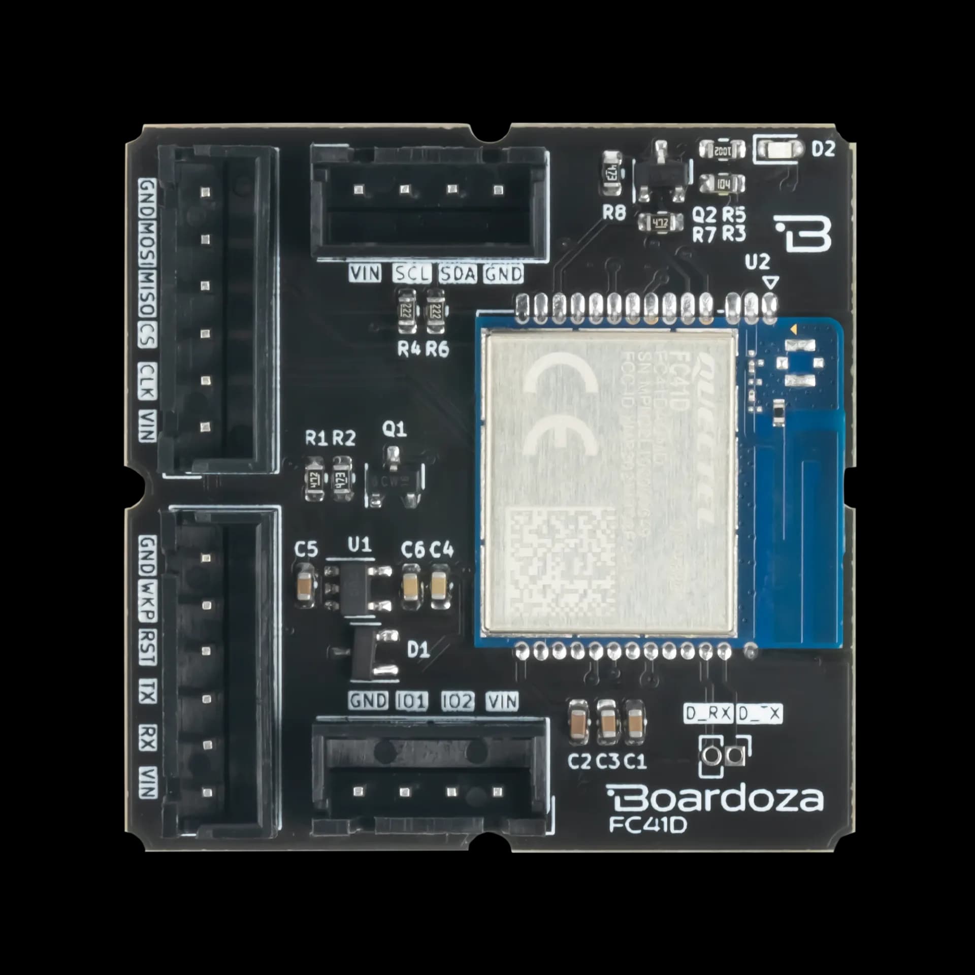
Boardoza Quectel FC41D Wi-Fi And Bluetooth Module Breakout Board
The Boardoza Quectel FC41D Module is a versatile wireless connectivity solution that combines Wi-Fi (802.11 b/g/n) and Bluetooth Low Energy (BLE 5.2) protocols into a single compact module. Designed for IoT, smart home, and industrial wireless applications, this module provides seamless integration with a wide range of microcontrollers through UART, SPI, and I2C interfaces. Operating in the 2.4 GHz frequency band, the FC41D ensures wide compatibility and reliable performance in common network environments. Built-in security protocols such as WPA-PSK/ WPA2-PSK/ WPA3-SAE help maintain secure wireless communication.
Where to buy?


1 / 3
Product Details
Key Features
- Dual Protocol Support: Integrates both Wi-Fi (802.11 b/g/n) and Bluetooth 5.2 Low Energy.
- Flexible Interface Options: Offers UART, SPI, and I2C for easy connection with various host systems.
- Secure Wireless Communication: Supports WPA-PSK/ WPA2-PSK/ WPA3-SAE standards for protected data exchange.
- Standard Frequency Range: Operates in the 2.4 GHz ISM band, widely used in IoT and wireless consumer products.
- Optimized for IoT: Ideal for devices requiring low-to-moderate data transfer rates such as smart sensors, wearables, and automation systems.
Technical Specifications
- Model
- Quectel FC41D Input
- Voltage
- 5V Voltage Input
- Type
- Multiple 4–6 pin headers (standard 2.50mm pitch)
- Functions
- Wi-Fi & Bluetooth Module
- Protocols
- WPA-PSK/ WPA2-PSK/ WPA3-SAE
- Band
- 2.4 GHz ISM band
- Interface
- I2C, UART, SPI
- Temperature
- -40°C to +85°C
- Dimensions
- 40mm x 40mm
Board Pinout
Debug Connector
| Pin Number | Pin Name | Description |
|---|---|---|
| 1 | D_TX | Debug TX Input |
| 2 | D_RX | Debug RX Input |
( J3 ) SPI Connector
| Pin Number | Pin Name | Description |
|---|---|---|
| 1 | VIN | Voltage Input |
| 2 | CLK | SPI Clock Pin |
| 3 | CS | Chip Select Pin |
| 4 | MISO | SPI MISO Pin |
| 5 | MOSI | SPI MOSI Pin |
| 6 | GND | Ground |
( J4 ) UART Connector
| Pin Number | Pin Name | Description |
|---|---|---|
| 1 | VIN | Voltage Input |
| 2 | RX | UART Receive Pin |
| 3 | TX | UART Transmit Pin |
| 4 | RST | Reset Pin |
| 5 | WKP | Wake-Up Pin |
| 6 | GND | Ground |
( J5 ) I2C Connector
| Pin Number | Pin Name | Description |
|---|---|---|
| 1 | VIN | Voltage Input |
| 2 | SCL | I2C Serial Clock Pin |
| 3 | SDA | I2C Serial Data Pin |
| 4 | GND | Ground |
Datasheet
Download (PDF)Support
For technical questions, documentation and issue reports, use the GitHub repository or write to us directly.