
Boardoza PC817C 4CH Isolated Level Shifter Breakout Board
The Boardoza PC817C 4CH Isolated Level Shifter Breakout Board is a high-quality isolation and voltage level translation module based on the Sharp PC817C optocoupler. Designed with four independent signal channels, it enables safe and effective communication between circuits operating at different voltage levels, offering complete galvanic isolation for each channel. The module supports both 3.3V and 12V logic levels on the input and output sides, making it suitable for a wide variety of applications, including signal isolation, industrial automation, PLC communication, and microcontroller logic interfacing. Its ability to operate up to 1.5 kHz ensures reliable digital signal transfer while maintaining signal integrity.
Where to buy?


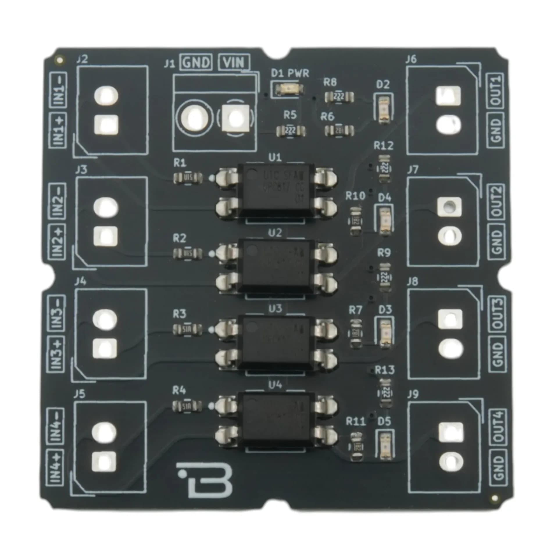
Key Features
- Four Independent Channels: Each signal channel is fully isolated using Sharp PC817C optocouplers.
- Wide Voltage Range: Compatible with 3.3V to 12V logic systems on both input and output sides.
- Safe Signal Conversion: Provides reliable galvanic isolation between low and high voltage domains.
- Unidirectional Transmission: Ideal for logic level shifting and digital signal interfacing.
Technical Specifications
- Model
- Sharp PC817C
- Manufacturer
- Sharp Corporation
- Functions
- Isolated Logic Level Shifting
- Channels
- 4
- Input Voltage Range
- 3.3V – 12V
- Input Current (per channel)
- ≤ 60 mA
- Output Voltage Range
- 3.3V – 12V
- Output Current (per channel)
- ≤ 50 mA
- Maximum Frequency
- 1.5 kHz
- Variation
- ≤ 60 mA
- Operating Temperature
- 3.3V – 12V
- Dimensions
- 1.5 kHz
Board Pinout
( J1 ) Power Supply
| Pin Number | Pin Name | Description |
|---|---|---|
| 1 | VIN | Voltage supply pin for output signal voltage level |
| 2 | GND | Reference ground of the signal output channels |
( J2 ) Input Channel 1
| Pin Number | Pin Name | Description |
|---|---|---|
| 1 | IN1+ | External signal input for Channel 1 |
| 2 | IN1- | Return ground for Channel 1 input |
( J3 ) Input Channel 2
| Pin Number | Pin Name | Description |
|---|---|---|
| 1 | IN2+ | External signal input for Channel 2 |
| 2 | IN2- | Return ground for Channel 2 input |
( J4 ) Input Channel 3
| Pin Number | Pin Name | Description |
|---|---|---|
| 1 | IN3+ | External signal input for Channel 3 |
| 2 | IN3- | Return ground for Channel 3 input |
( J5 ) Input Channel 4
| Pin Number | Pin Name | Description |
|---|---|---|
| 1 | IN4+ | External signal input for Channel 4 |
| 2 | IN4- | Return ground for Channel 4 input |
( J6 ) Output Channel 1
| Pin Number | Pin Name | Description |
|---|---|---|
| 1 | OUT1 | Converted signal output for Channel 1 |
| 2 | GND | Output reference ground for Channel 1 |
( J7 ) Output Channel 2
| Pin Number | Pin Name | Description |
|---|---|---|
| 1 | OUT2 | Converted signal output for Channel 2 |
| 2 | GND | Output reference ground for Channel 2 |
( J8 ) Output Channel 3
| Pin Number | Pin Name | Description |
|---|---|---|
| 1 | OUT3 | Converted signal output for Channel 3 |
| 2 | GND | Output reference ground for Channel 3 |
( J9 ) Output Channel 4
| Pin Number | Pin Name | Description |
|---|---|---|
| 1 | OUT4 | Converted signal output for Channel 4 |
| 2 | GND | Output reference ground for Channel 4 |
Datasheet
Download (PDF)Support
For technical questions, documentation and issue reports, use the GitHub repository or write to us directly.