
Boardoza M032KG Educational Development Kit
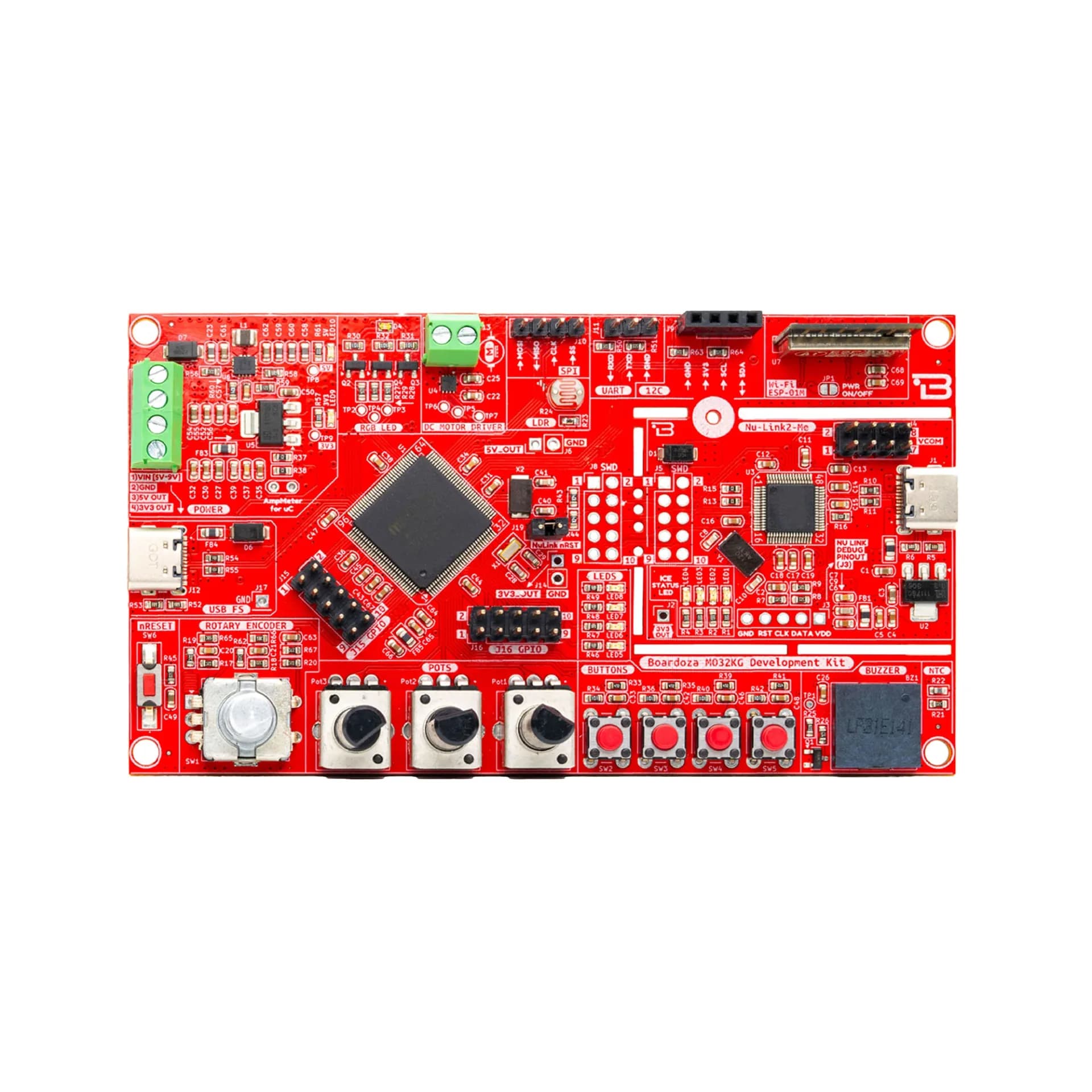
The Boardoza M032KG is a comprehensive educational development kit designed around the Nuvoton M032KG8AE platform. It integrates a M032 microcontroller and a Nu-Link2-Me-compatible debugger and programmer, offering a complete environment for embedded development, learning, and rapid prototyping. Inspired by the Nuvoton Nu-Link2-Me, this board is fully compatible with Nu-Link debugging tools and workflows, providing seamless integration with existing toolchains. It supports on-board debugging, virtual COM (VCOM), power measurement, and modular expansion.
Where to buy?


Product Details
This versatile kit includes a rotary encoder, potentiometers, a buzzer, an RGB LED, an NTC thermistor, an LDR, a DC motor driver, user LEDs and buttons, an OLED display interface, an ESP-01M Wi-Fi module header, and various other peripherals. These features make it ideal for education, experimentation, prototyping, and IoT application development.
Key Features
- M032KG8AE MCU with 20 GPIO breakout header
- Compatible with Nu-Link2-Me: Integrated on-board debugger & programmer
- On-board Virtual COM Port (VCOM) support
- Power measurement header for ammeter connection
- OLED screen connector for UI/graphic development
- ESP-01M (Wi-Fi) header
- On-board peripherals: Rotary encoder, potentiometer, user LEDs & buttons, NTC, LDR, buzzer, RGB LED
- DC motor driver outputs
- USB Type-C for data/power, external 5–9V input support
- Multi-interface pinouts (1xUART, 1xI2C, 1xSPI)
Technical Specifications
- Model
- Boardoza M032KG Development Board
- MCU Core
- Nuvoton M032KG8AE
- Input Voltage
- 5V – 9V (via terminal block connector)
- USB Interface
- USB Type-C (data and power)
- Debugger
- Nu-Link2-Me Compatible
- Operating Temperature
- -25°C ~ +85°C
- Board Dimensions
- 68mm x 116mm
- Mounting Holes
- 4 × M3
Board Pinout
ESP-01M Wi-Fi Power Jumper (JP1)
| Pin Number | Pin Name | Description |
|---|---|---|
| 1-2 | OPEN | ESP-01M Wi-Fi module power not active (default) |
| 1-2 | SHORT | ESP-01M Wi-Fi module power enabled |
( J6 ) 5V Power Output
| Pin Number | Pin Name | Description |
|---|---|---|
| 1 | 5V | 5V Output |
| 2 | GND | Ground |
( J14 ) 3.3V Power Output
| Pin Number | Pin Name | Description |
|---|---|---|
| 1 | 3V3 | 3.3V Output |
| 2 | GND | Ground |
( J18 ) Mixed Voltage Terminal
| Pin Number | Pin Name | Description |
|---|---|---|
| 1 | VIN | External Power Input (5V–9V) |
| 2 | GND | Ground |
| 3 | 5V | 5V Output |
| 4 | 3V3 | 3.3V Output |
Debug Power Selection Jumper (J19)
| Pin Number | Pin Name | Description |
|---|---|---|
| 1-2 | OPEN | Use USB from MCU side (default) |
| 1-2 | SHORT | Enable Nu-Link2-Me debugger connection |
Motor Driver Output (J13)
| Pin Number | Pin Name | Description |
|---|---|---|
| 1 | OUT1 | DC Motor Output |
| 2 | OUT2 | DC Motor Output |
SWD Debug Header (J8)
| Pin Number | Pin Name | Description |
|---|---|---|
| 1 | NC | Not Connected |
| 2 | VCC | Positive Supply |
| 3 | NC | Not Connected |
| 4 | DATA | SWD Data I/O |
| 5 | NC | Not Connected |
| 6 | CLK | SWD Clock |
| 7 | MCU_TX | MCU UART TX (PB.13) |
| 8 | nRST | MCU Reset |
| 9 | MCU_RX | MCU UART RX (PB.12) |
| 10 | VSS | Ground |
I2C Connector (J9)
| Pin Number | Pin Name | Description |
|---|---|---|
| 1 | GND | Ground |
| 2 | 3V3 | Power |
| 3 | SCL | I2C0 PE.13 |
| 4 | SDA | I2C0 PC.8 |
SPI Connector (J10)
| Pin Number | Pin Name | Description |
|---|---|---|
| 1 | SS | SPI0 PA.3 |
| 2 | CLK | SPI0 PA.2 |
| 3 | MISO | SPI0 PA.1 |
| 4 | MOSI | SPI0 PA.0 |
UART Connector (J11)
| Pin Number | Pin Name | Description |
|---|---|---|
| 1 | RXD | UART4 PC.6 |
| 2 | TXD | UART4 PC.7 |
| 3 | GND | Ground |
( J15 ) GPIO Group A
| Pin Number | Pin Name | Description |
|---|---|---|
| 1 | PE.7 | Multi-Function |
| 2 | PE.6 | Multi-Function |
| 3 | PE.5 | Multi-Function |
| 4 | PE.4 | Multi-Function |
| 5 | PH.8 | Multi-Function |
| 6 | PH.9 | Multi-Function |
| 7 | PB.10 | Multi-Function |
| 8 | PB.11 | Multi-Function |
| 9 | PB.8 | Multi-Function |
| 10 | PB.9 | Multi-Function |
( J16 ) GPIO Group B
| Pin Number | Pin Name | Description |
|---|---|---|
| 1 | PA.10 | Multi-Function |
| 2 | PB.0 | Multi-Function |
| 3 | PA.8 | Multi-Function |
| 4 | PA.9 | Multi-Function |
| 5 | PD.11 | Multi-Function |
| 6 | PD.12 | Multi-Function |
| 7 | PG.2 | Multi-Function |
| 8 | PD.10 | Multi-Function |
| 9 | PF.9 | Multi-Function |
| 10 | PF.10 | Multi-Function |
( J2 ) Power Output
| Pin Number | Pin Name | Description |
|---|---|---|
| 1 | 3V3 | 3.3V Output |
( J5 ) SWD/ICE Debug Connector
| Pin Number | Pin Name | Description |
|---|---|---|
| 1 | VCC | Power |
| 2 | NC | Not Connected |
| 3 | DATA | SWD Data I/O |
| 4 | NC | Not Connected |
| 5 | CLK | SWD Clock |
| 6 | NC | Not Connected |
| 7 | nRESET | Reset Line |
| 8 | ICE_RX | Debugger UART RX |
| 9 | VSS | Ground |
| 10 | ICE_TX | Debugger UART TX |
( J4 ) UART Jumper Settings
| Pin Number | Pin Name | Description |
|---|---|---|
| 1-2 | TXD | Connect PB.13 (UART0_TXD) to debugger |
| 3-4 | RXD | Connect PB.12 (UART0_RXD) to debugger |
| 5-6 | MSG EN | Enable/disable Virtual COM messages |
| 7-8 | NC | Not Connected |
Support
For technical questions, documentation and issue reports, use the GitHub repository or write to us directly.